(Mini Mutable Yarns open-source build and overview)
Resources:
- Bill of Materials (BOM) Spreadsheet
- Original Yarns Schematic (also useful – manual and quickstart)
- Firmware on Google Drive (zip)
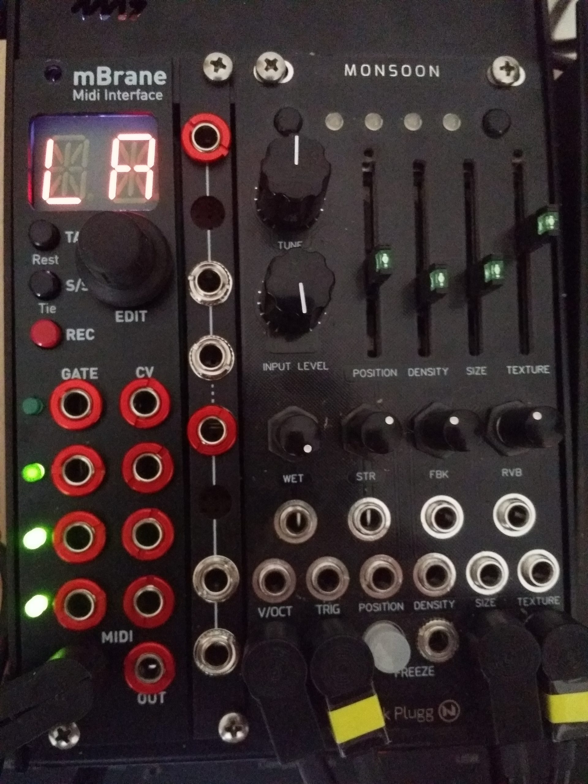
After getting comfortable with using the Jakplugg monsoon (12hp expanded Mutable Clouds), I started looking around for a midi-to-cv module to control the pitch and clock of the monsoon and modulate some of the parameters. I briefly considered a few other small modules like the Befaco Midi Thing, but eventually settled on the mbrane because of the small, skiff-friendly size, 16-bit DAC, and open-source code base. In theory, if I want to add some features later, re-compiling the firmware should not be terribly difficult. Built mbranes are extremely difficult to come by though
I didn’t see a build guide for the module posted anywhere online. The assembly and programming is a bit complex, and the BOM a bit out of date, so I’ve decided to write up my experiences putting the thing together. Hopefully it can help someone decide if its the right project to take on.
1. Parts
The bill of materials posted from pusherman, where I got the board and panel, is a useful place to start, but lists a number of parts that are obsolete or aren’t regularly stocked at Mouser. The spreadsheet for my order is page 1 in the above xls spreadsheet (the original Jakplugg Google BOM is page 3). Mouser has a nice BOM upload tool that should auto-add all the needed parts unless some more go out of date in the meantime. Note a few things in my updated BOM:
- The encoder is the non-threaded version, as the listed part had about a minimum 2 month lead time. I recommend the threaded one in the original BOM if available. The board is pretty sturdy as-is, but I will probably change it out at some point to have the attachment point to the panel.
- The display I got is red (to match the vanity red jack nuts of course!), though the build calls for green. Any color in the same series should work, but I would be careful with some of the high-intensity versions.
- The switches in my BOM are specced as requiring a slightly lower pressing force. This doesn’t matter, it was down to what they had in stock.
The 2 stereo and 8 mono jacks from Thonk came speedily, along with a 16-to-10 pin power cable. The standard pitch (2.54mm) header pins and a 1.27mm 2×5 socket for knocking together a programmer cable came from the local electronics store GME since they’re cheap and I get a bunch at once there.
In addition to this, I got a generic “Mini ST-Link V2” USB programmer for about $5 off ebay, available in the color of your choice. It worked fine for uploading the bootloader and firmware (below).
2. Soldering
This wasn’t my absolute first SMD rodeo, but most previous projects have been limited to a SOIC here and there or adapter boards. The microprocessor LQFP48 looked pretty intimidating initially. I made sure to watch a number of ‘SMD practice’ videos, but the basic steps below with some adaptation, lots of testing, and lots of flux, worked for me.
Equipment
Soldering iron: Can’t get very far without this; below is my basic 48W iron. It’s not an expensive one, about $20 here, but temperature control is important. I tested with my solder and reduced the temperature as much as possible while still maintaining a shiny, oxidation-free tip and fast melt rate. The setting here is the one I largely used (just below the ‘line’ between 300 and 350 C) but I doubt the printed values are very accurate.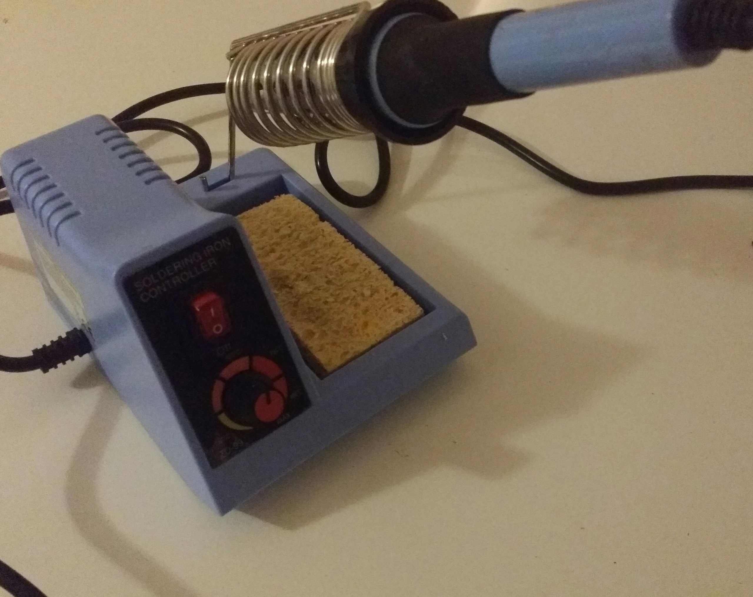
Soldering Accessories: For the tip, I sanded down the comically huge one it came with to a not-quite-sharp chisel tip and then gave it a good scrub with a clean steel pot scrubber before tinning. The image below is the re-sharpened tip after doing all the soldering (before re-tinning). I also re-sharpened once during the build, just before doing the microprocessor. Sharpening like this probably isn’t the ideal method, since the inside and outside of the tip are different metals, and the inner metal is very soft and tends to wear out. But I have a few alternate tips for the iron for normal work, so I didn’t mind scrapping this one. It worked out advantageously though – solder tended to pool in a ball in the middle of the chisel, while the outer edges could be used to re-flow with precision.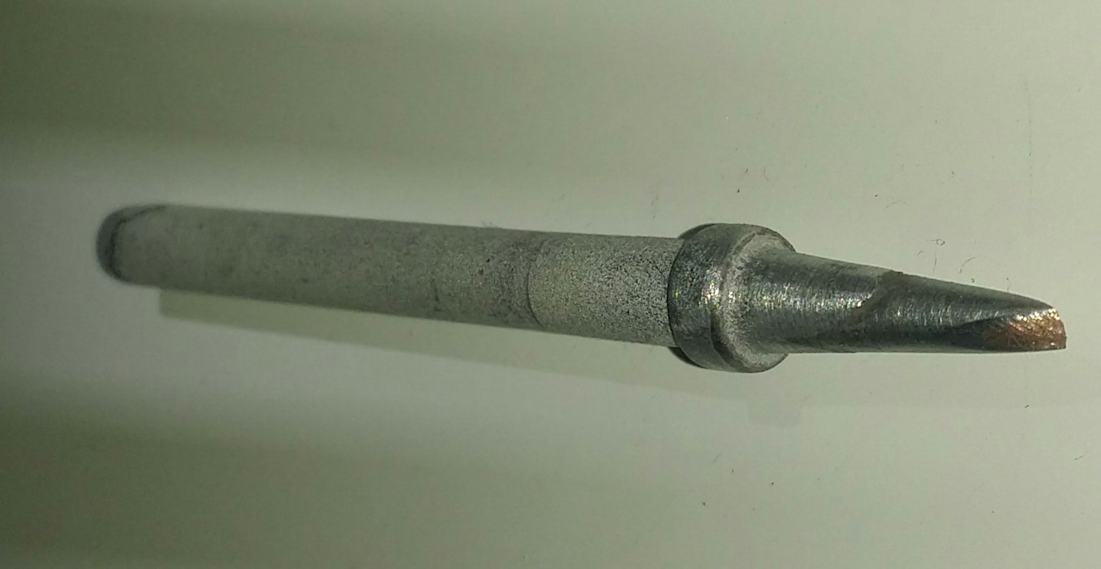
Other necessary accessories (below) were a solder spool (as thin as practically possible), liquid flux and flux pen, tweezers and a non-metallic stick for pushing things around, tip tinner, and cleaning tools – alcohol (90% Isopropanol), a brush, and distilled water (for the sponge, and for rinsing off the alcohol and flux). Also a digital multimeter to make sure all the soldering does what you intended and nothing you didn’t. The razor I pretty much just used for opening the tape packaging most of the parts were in.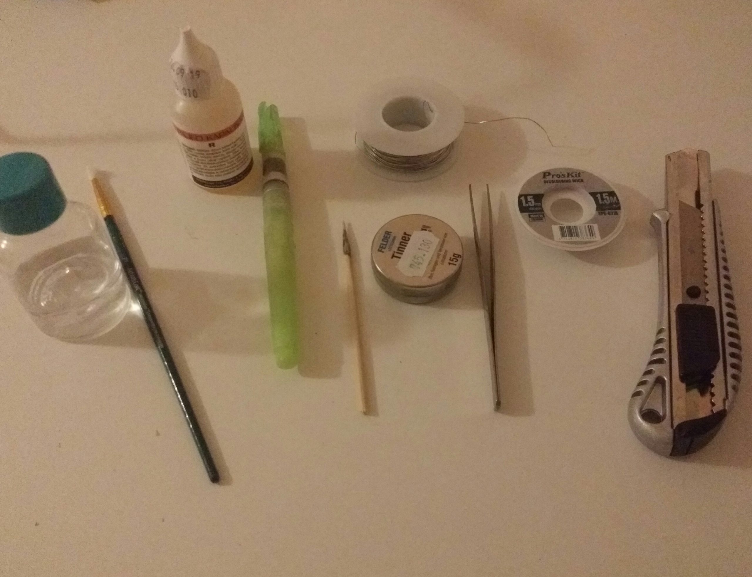
I did not use a grounding strap, but I wiped the tweezers on a grounded wire before handling anything that came in a shiny foil bag with them. It has been somewhat humid here in the Summer, and I don’t have a synthetic carpet in the work room. If there is a lot of dryness/plastics around or you get an occasional static zap where you plan to solder, get a strap. I also have some desolder braid, but it is coarse and kind of crappy for fine work. I used it to clean up a couple of lazy spots on the through-hole components but did not rely on it for the SMD work. I would recommend having some nice, fine desolder braid around though to make life easier.
Oh, and a good lamp. I do not (knock on wood) quite need a magnifying glass yet to see most of these tiny things, but a super bright lamp is absolutely critical to the process.
Process
Most of the parts can be placed by matching the BOM to the printed PCB, but this is NOT comprehensive. To place parts, I worked through the BOM, and pulled up the original Yarns schematic (linked above) if I had any doubts, and then went to datasheets if I still had any doubts. I had many doubts, since a lot of things are not documented on the PCB printing or the BOM, and even from these markings, many were illegible: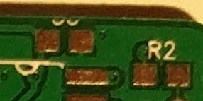
That turned out to be ‘C6’ in the upper-left corner. I left that for last, just to be sure.
In general, I started with the resistors – harder to screw up, and easier to test with a multimeter in case anything was going wrong with my process. The small (ceramic) capacitors were next, then the ICs, then the 4 electrolytic capacitors, then the mini-JTAG connector (the 2×5 row with 1.27mm spacing). Then, after programming, the remaining through-hole components.
My method for attaching most of the SMD components was the same:
- i. Clean area with alcohol and brush. Let dry, flux.
- ii. Put a thin layer of solder on one board pad only.
- ii. Hold component in place and re-flow that pad until it holds.
- iii. *Gently* push down on the top of the component with tweezers and reflow the pad again to set flat.
- iv. Flux everything again.
- v. Solder the other pad(s) normally, then re-flow the first one and add more solder if necessary.
For the ICs with lots of leg (more than 3), instead of pre-soldering the pad, it was better to simply set the component flat and ‘tack’ one corner, and then (after checking and double-checking the alignment), soldering the remaining legs. This usually took another intermediary round of flux and reflow to make sure everything was down. Even so, and testing as much as I could as I went, I missed a couple spots on the ICs, but these were easy to fix later.
Orientation
A few notes on the parts that require a certain, non-obvious orientation, or not:
- The resistors and small ceramic capacitors can be put down in any orientation. The orientation of the electrolytic capacitors is easy to read from the board, just align the beveled edge with the diagram.
- There is a single 1N4148 Diode at the bottom of the board for the MIDI input. The line on the SMD package goes on the same side as the line on the diode icon (printed helpfully on the PCB) that denotes the cathode.
- The IC’s are mostly self-explanatory, except on the board most of the diagrams show the half-circle cutout that is standard for through-hole DIPs (with the #1 leg at the lower-left corner if the cutout is on the left). The ICs I got all followed one of these conventions:
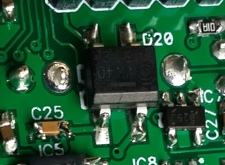
- i. If there is a line OR beveled edge on a side with legs, this is meant to be on the ‘bottom’. The #1 pin is then at the left end of this line or bevel. For example, here is the bridge diode. You can clearly see both the bevel and the pattern beneath it:
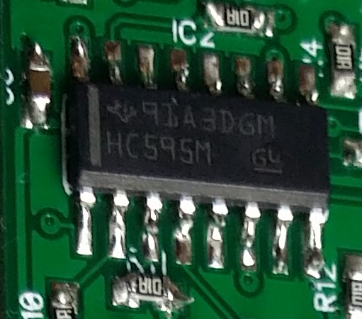
- ii. If there is a line on a side NOT with legs, this takes the place of the half-circle cutout. This is the case with, for example, the shift registers:
- If there is a ‘dot’ in a corner of the package, this goes in the lower-left, and is then above the #1 pin, but this is clearly indicated on the PCB printing.
- i. If there is a line OR beveled edge on a side with legs, this is meant to be on the ‘bottom’. The #1 pin is then at the left end of this line or bevel. For example, here is the bridge diode. You can clearly see both the bevel and the pattern beneath it:
- The Crystal Oscillator is a special case. This DOES have orientation, as it is not just a simple piezo. There is no indication of this on the PCB. Basically, there is a little printed number ’80’ frequency mark on one end of the package. This goes ‘down’ on the PCB. The board helpfully gives you no indication of this, I had to check datasheets to work it out:
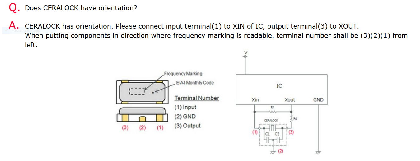
Great, so which are XIN and XOUT on the PCB?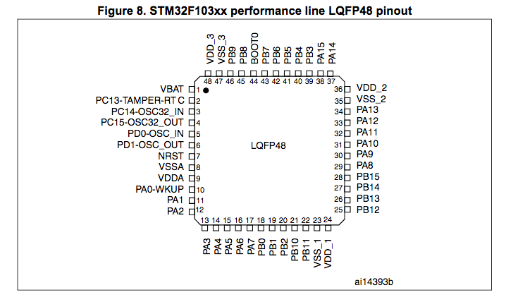
And from the original Yarns Schematic: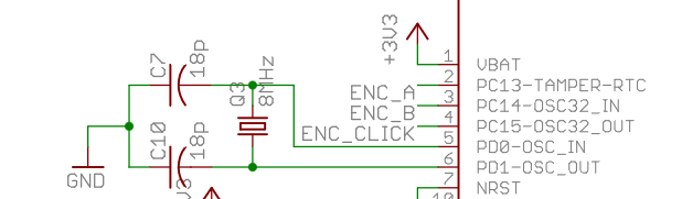
So, the end with the (’80’) connects to pin 6. Honestly, I had to use my phone camera and blow it up before I could read it, but it is the end of the package that scatters more light. The other end will look flat. Here it is, looking messy with lots of sticky flux: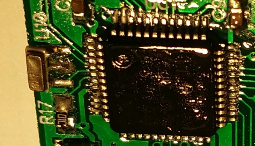
I also made the mistake of pre-soldering the top pad for the oscillator first, and then had a terrible time trying to get it to lie flat. I recommend fluxing everything, then placing it flat on the 3 pads, then tacking the MIDDLE contact and testing it before soldering the outer two.
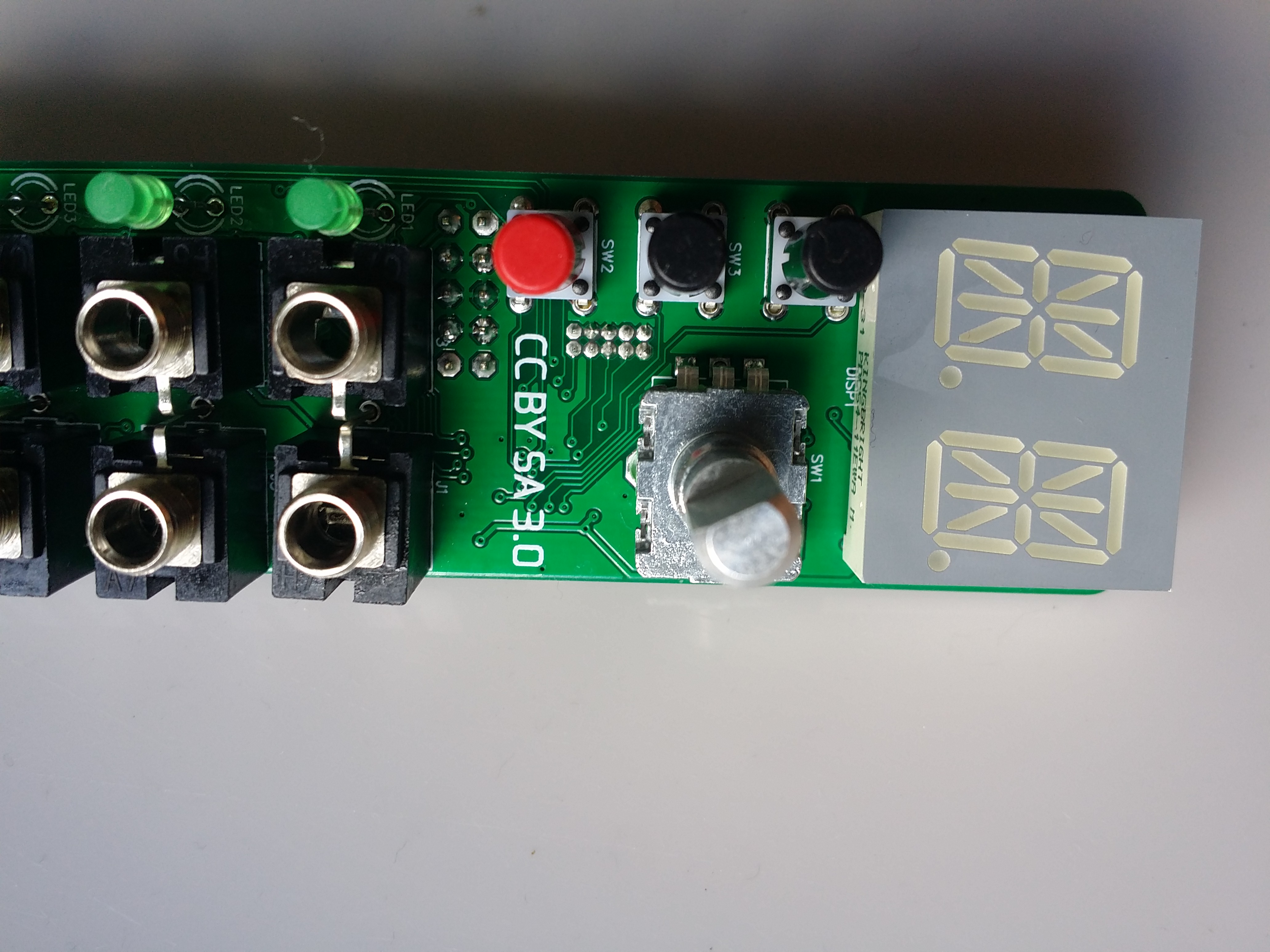
- The through-hole switches don’t have an orientation.
- The shorter (cathode) leg of the 4 through-hole LEDs go in the lower hole on the PCB. To check, these should all be wired together to ground (a multimeter will show all these points connected).
- The LED display fits into the PCB with the decimal points and the printed text down. Seems obvious, but I checked it anyway.
Soldering the Arm microprocessor was a special case. It is absolutely critical to make sure the legs are aligned with the pads. Especially on this PC board, there is almost no room for error, and a leg mis-alignment can botch the whole project. It would be very nice if, in future versions of the board, the pads were made a little longer since in this one, the legs come almost right up to the edge of the pads and make it very difficult to see if any solder has wetted on without a microscope.
Tacking the first IC leg so that the rest of the chip is aligned is absolutely the most critical step of the entire build. After this, I re-checked the STM alignment multiple times with every magnification tool I could muster (phone camera, girlfriend’s glasses, etc). Then I tacked the other 3 corners so that the first tack point would not bend or break the leg as I worked down the sides.
I have seen a ‘flood solder’ method recommended for chips like this. I did not use it. I don’t trust my desolder wick enough for that. What I did do is basically slightly over-solder the corners, flux the hell out of everything, and then ‘wipe’ the extra solder off the corner leg and then down the line of legs until everything looked about the same. Even so, at 2 points I had legs with a wad of solder between them that I removed by de-tinning the iron (vigorous wiping on the sponge), re-fluxing (again), and eventually, when it was absolutely necessary, flossing the sharpened ‘blade’ of the tip carefully between the legs to remove the excess solder. I don’t recommend this with anything but a knife-edge tip, honestly it would be much less nerve-wracking to just get the good desolder braid, flood-solder or no.
After that, I programmed the STM32F103 to make sure nothing had gone horribly wrong (the chip can be programmed with only the 3.3V from the ST-Link and if something IS wrong, its better not to have chunky through-hole components in the way when fixing). Then I finished up soldering the through-hole components and cleaned the flux off. This was done by brushing IPA into the components, then rinsing IPA over the board, then rinsing off the IPA-and-Flux liquid with distilled water and letting everything air-dry. It may be tempting to use a hair dryer to help the drying along, but this is risky for static charge sensitive devices. The whole build took about 20 hours spread out over 7 days or so, working very slowly and testing everything I could as I went.
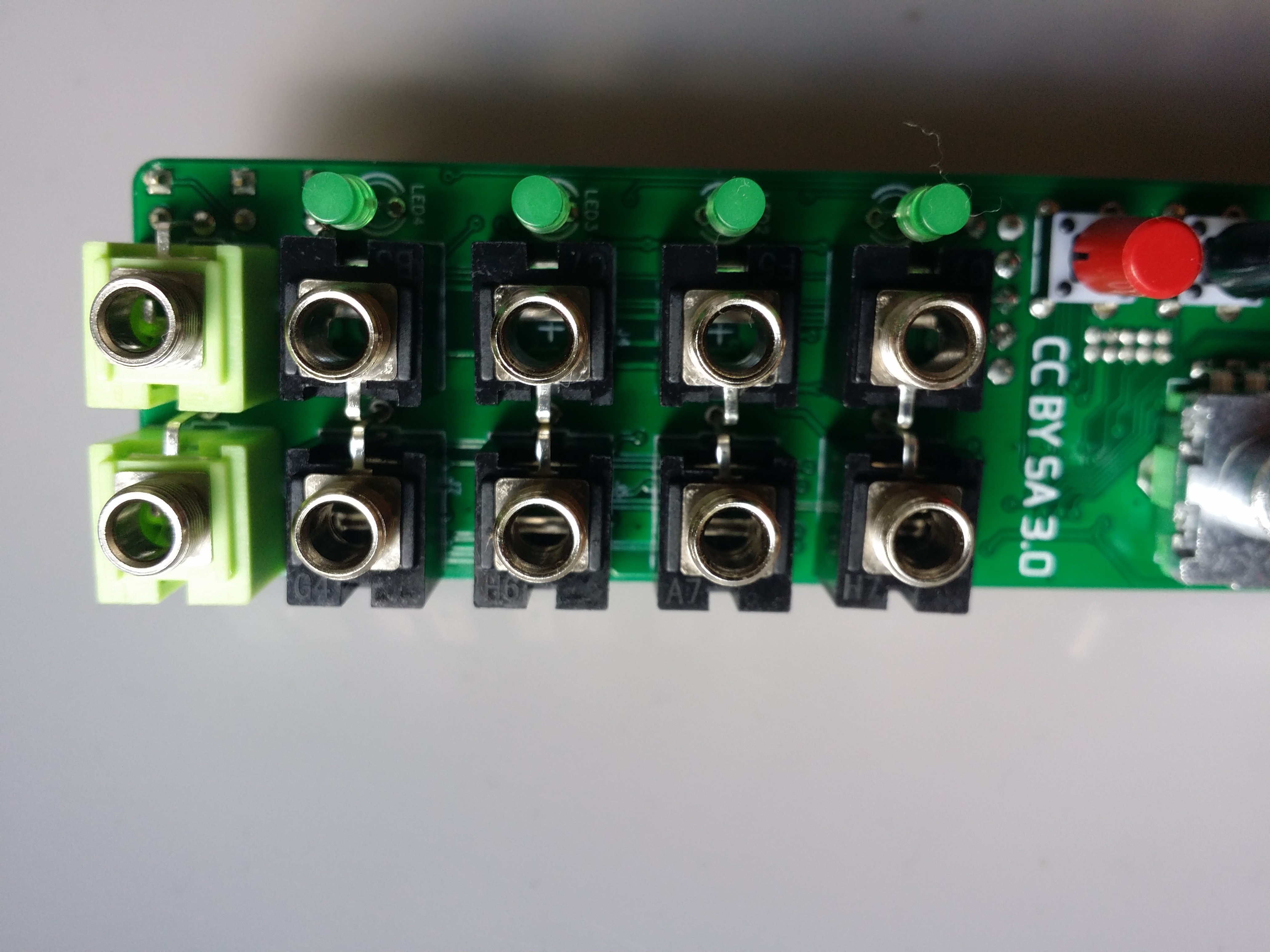
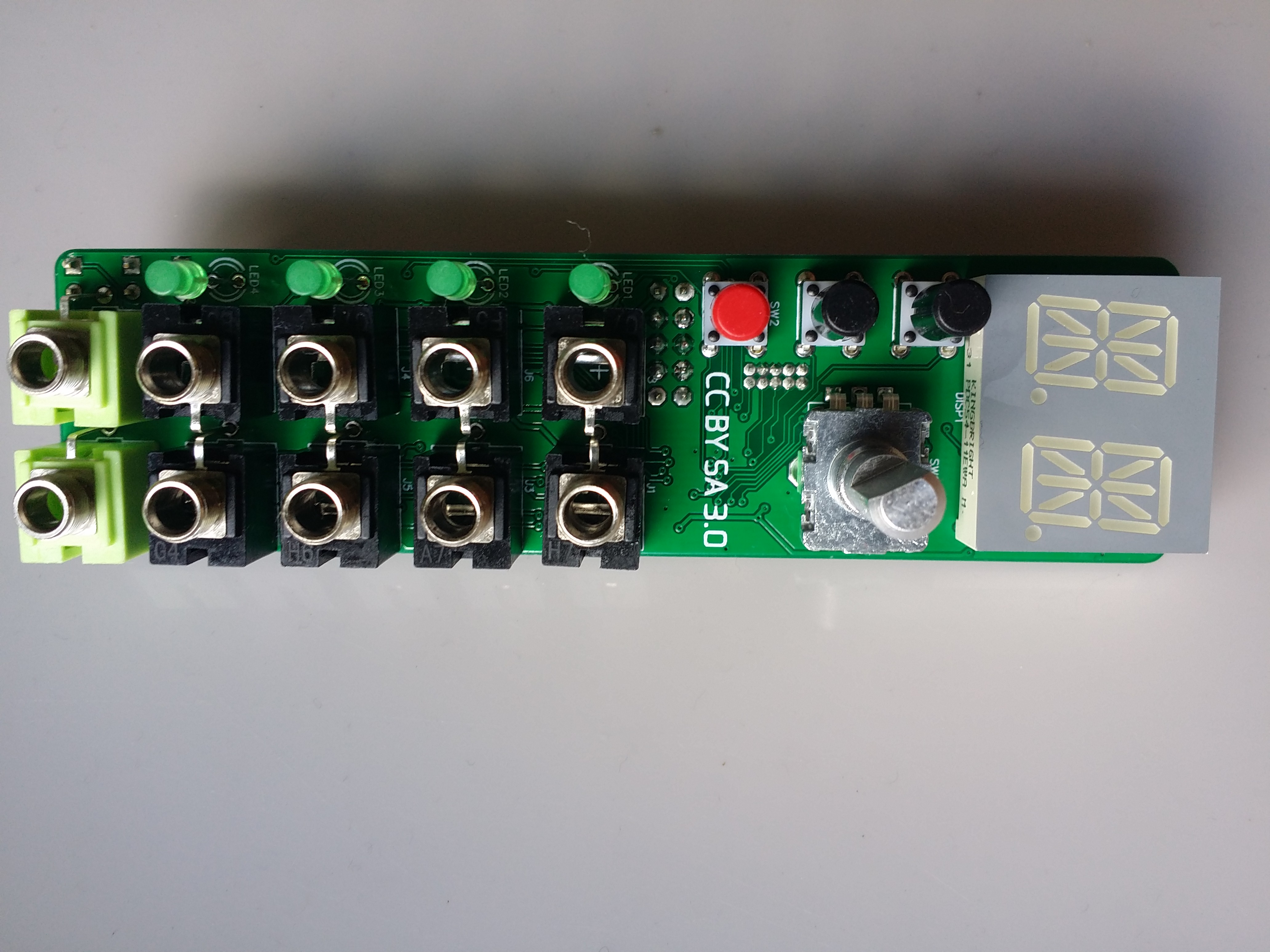
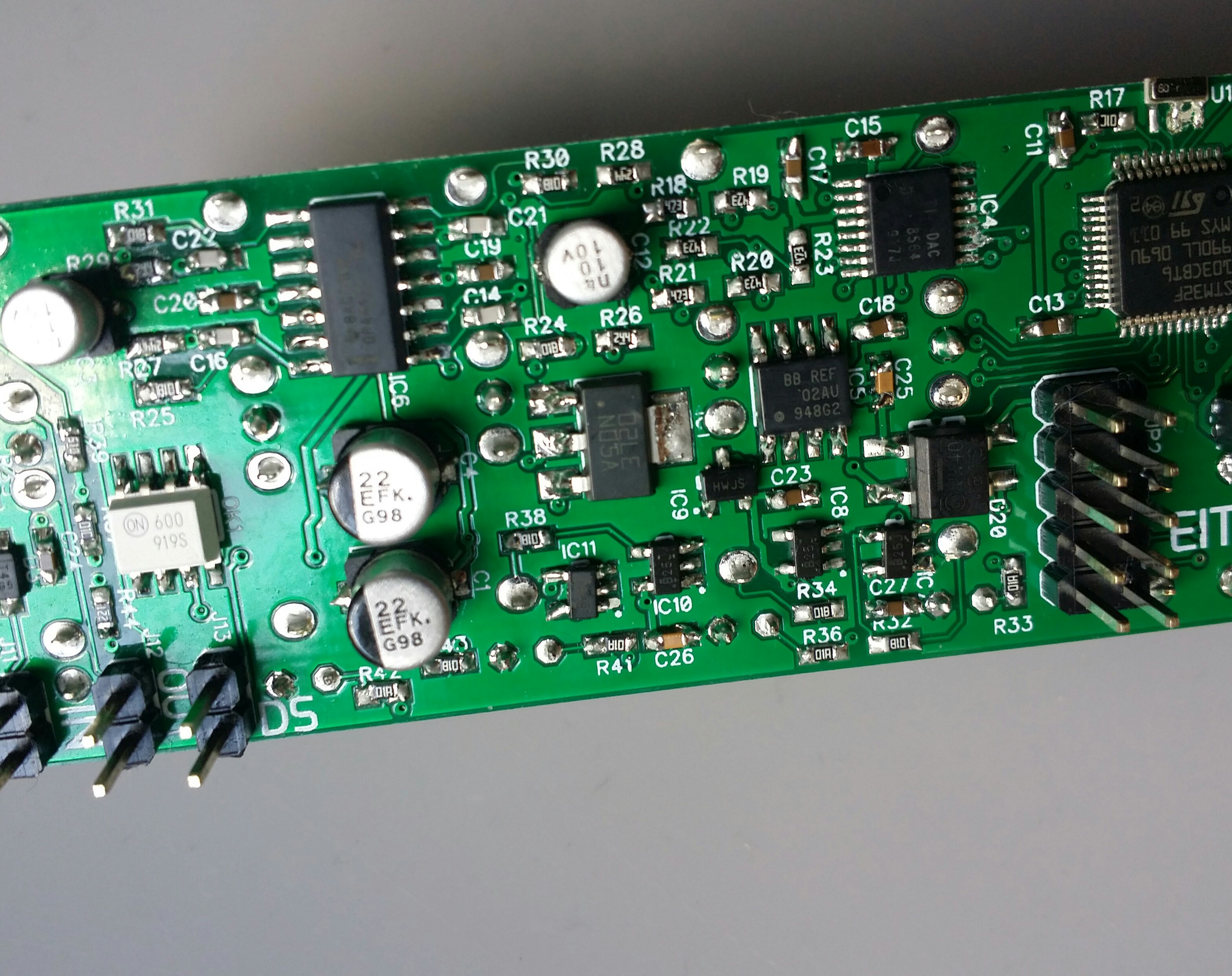
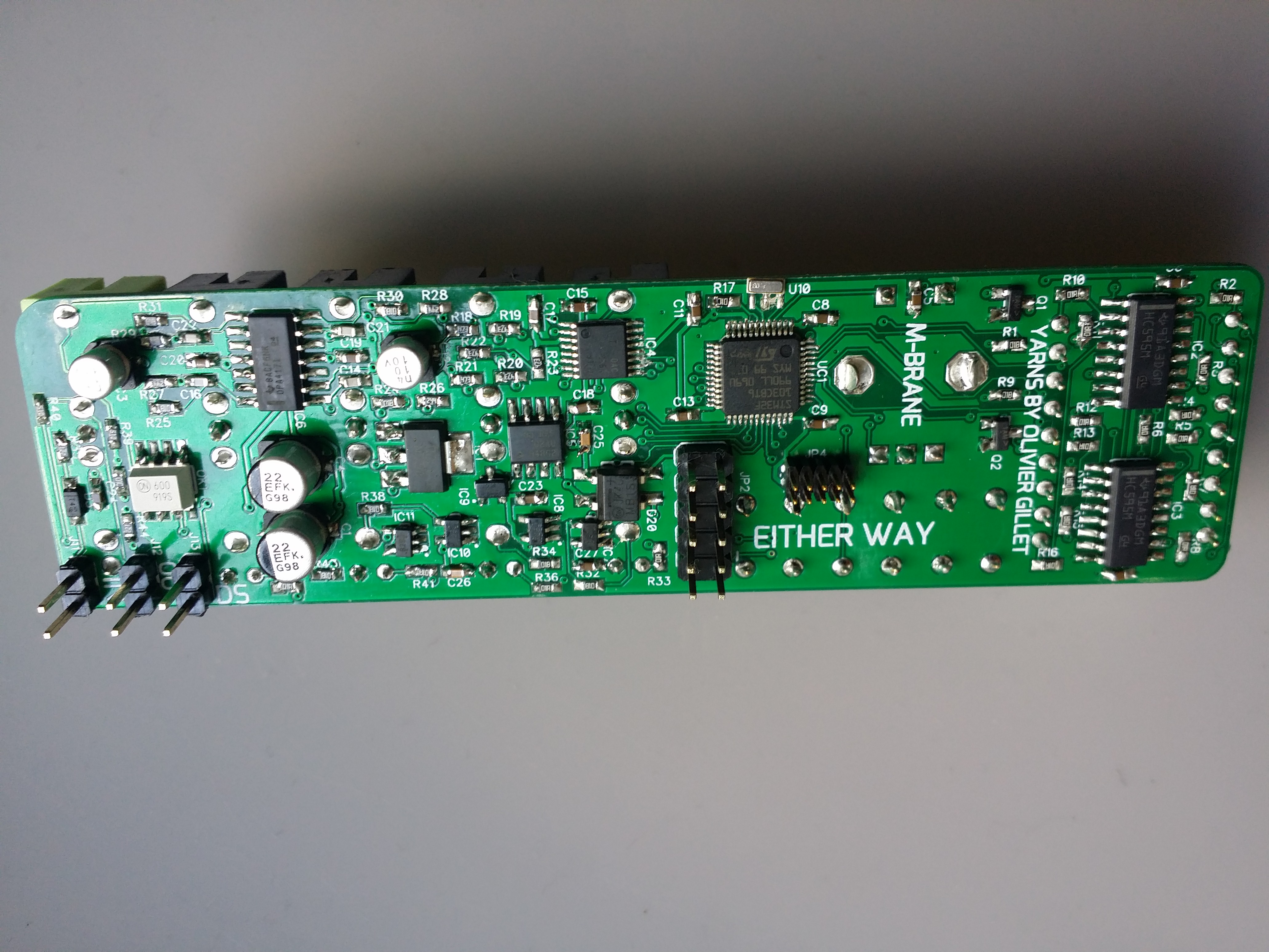
Full-scale images of the finished, cleaned-up board:
3. Programming
With everything soldered down, time to get the ARM programmed with the ST-Link V2. Downloaded ST-Link Utility, plugged in the cheapo USB ST-Link and updated the firmware. All of that worked fine. The next step was to get the right pins from the programmer to the mini-JTAG header. There are various ways to accomplish this, and lots of website will charge honestly absurd amounts to make sure the pins go to the right place. I just picked up a female 2×5 1.27mm pitch header from GME and soldered the wires from the programmer directly to it. (full disclosure: I bought 2 in case I broke a pin, which are very delicate. And I absolutely did!)
The Yarns schematic specifies five port connections to the microcontroller, but it only really needs three for the ST-LINK: SWDIO, SWCLK, and the Reset pin. The pins labeled ‘JTDO’ and ‘JTDI’, connecting to ports B3 and A15, respectively, can be left unconnected. Here’s the little sketch I worked it out on: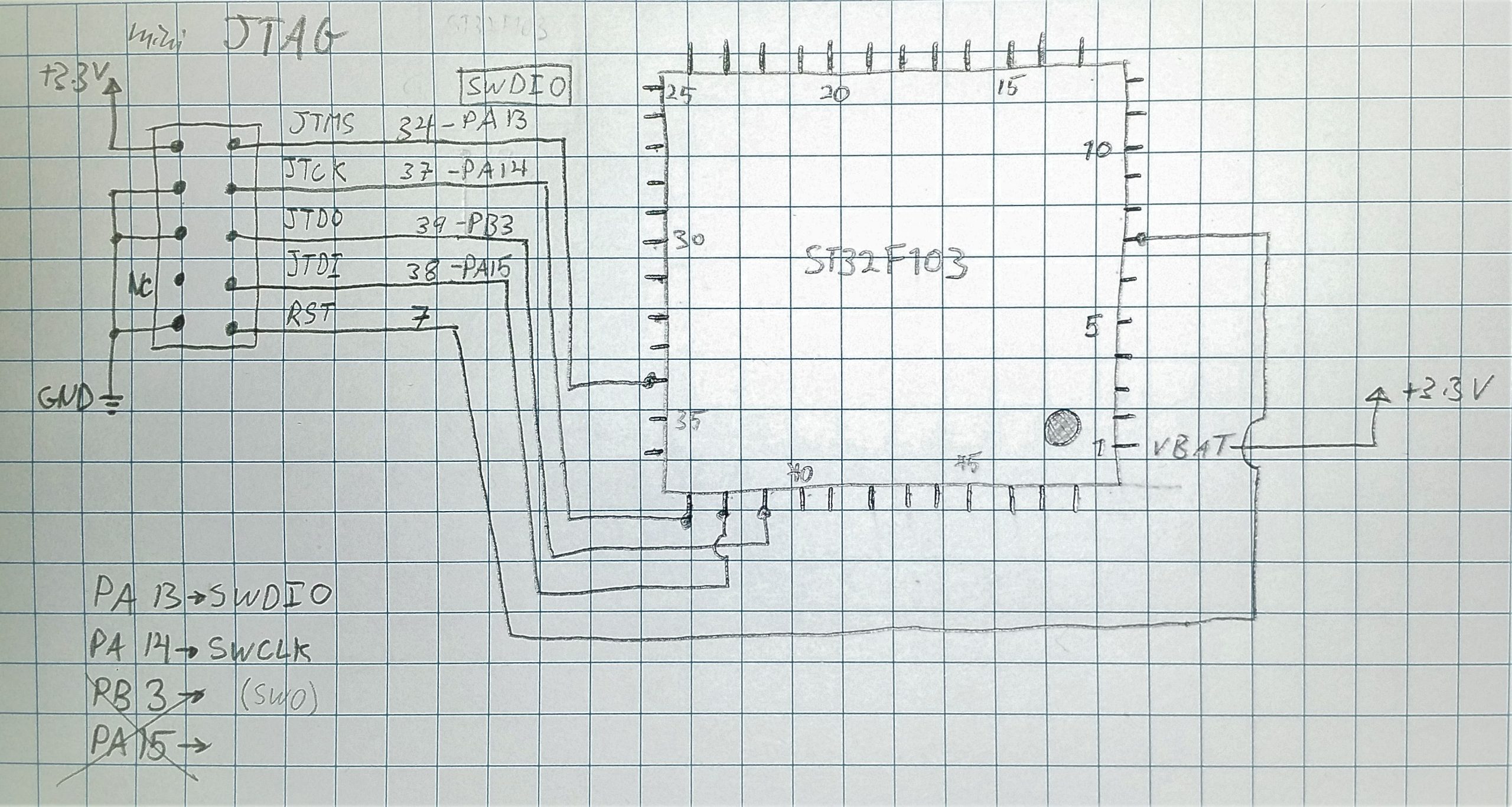
And the orientation on the board for reference: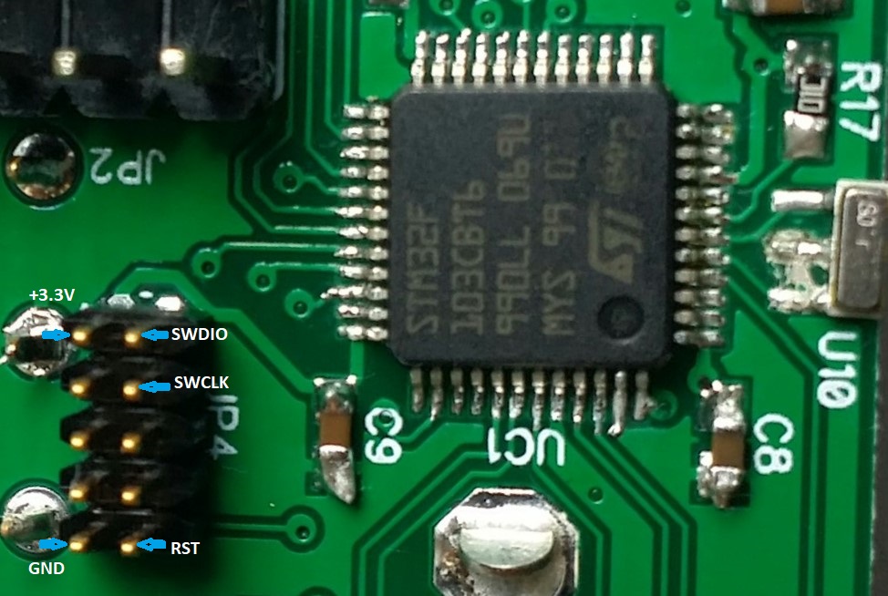
We need to hook up the +3.3V and ground, so there are 5 wires that need to go from the ST-LINK to the mini-JTAG header. Here’s my cludged-together mini-JTAG-to-USB adapter. The glue is nice, rubbery E6000 industrial adhesive to keep everything together: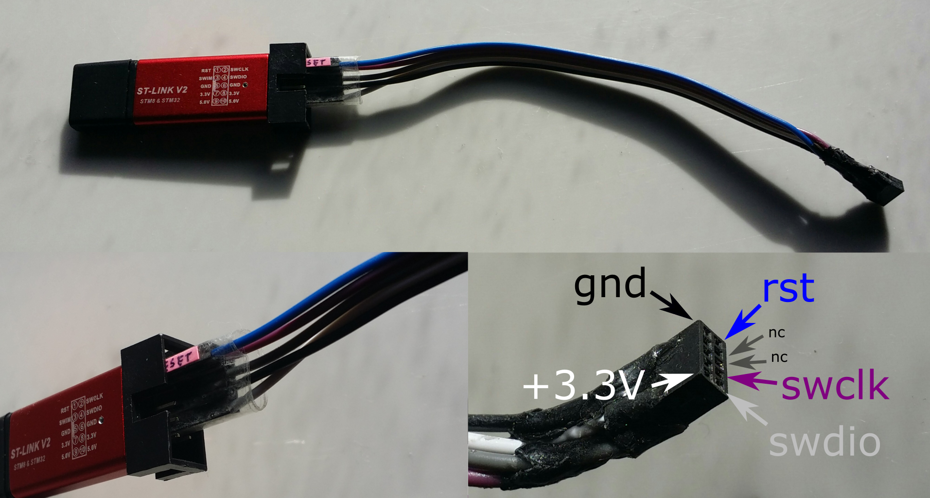
Actually loading the firmware was pretty much just plug-and-play. Select “Target > Connect”, then “Target > Program & Verify”. No other options were changed. The actual upload was on the order of tens of seconds. One note on the firmwares linked above: I had to upload yarns_bootloader.hex first, then I loaded Yarns_1.3.hex. Loading yarns.hex right off the bat initially did not work.
Here is everything happily connected and ready to be programmed in the ST-LINK Utility: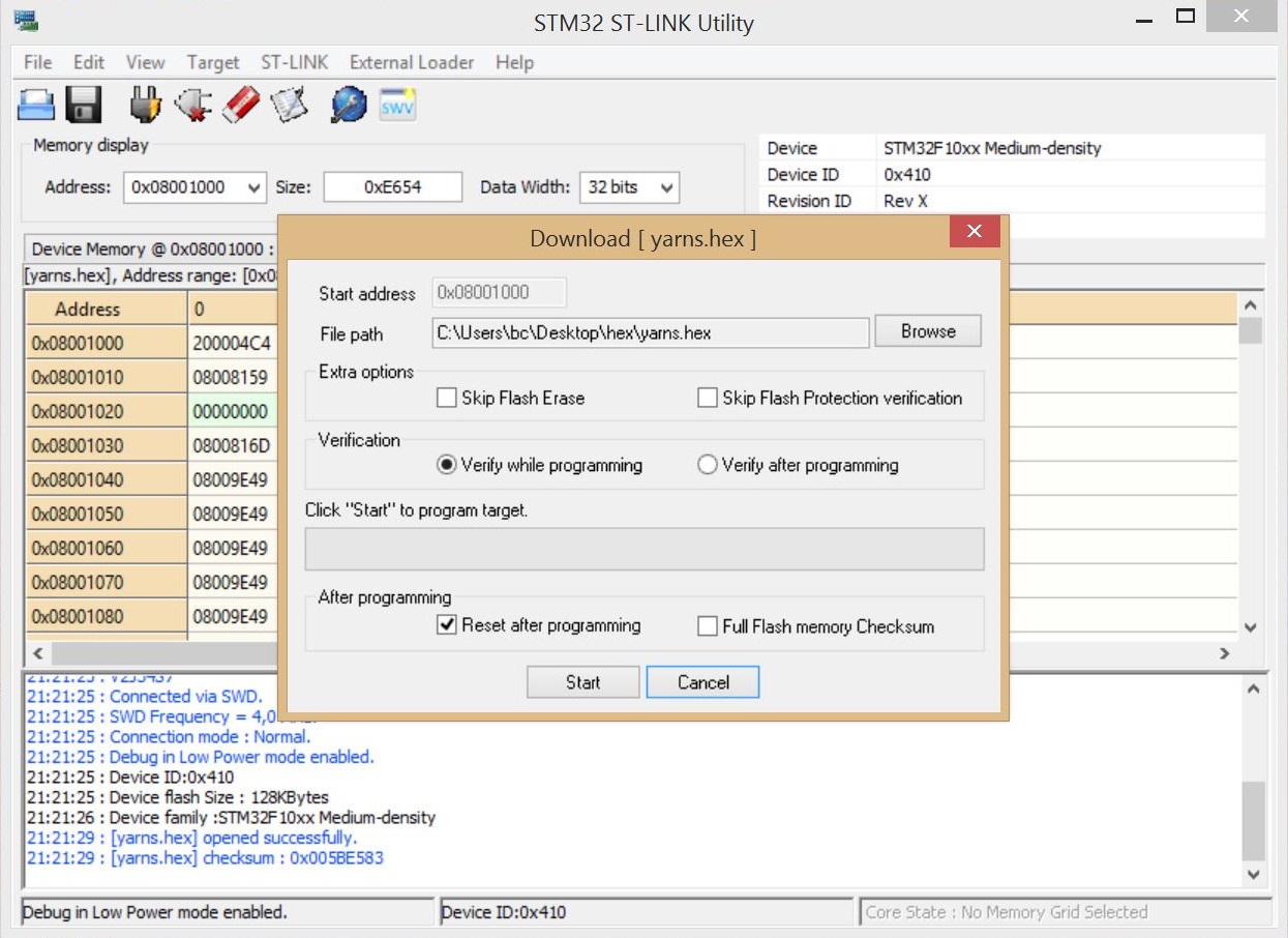
4. Troubleshooting
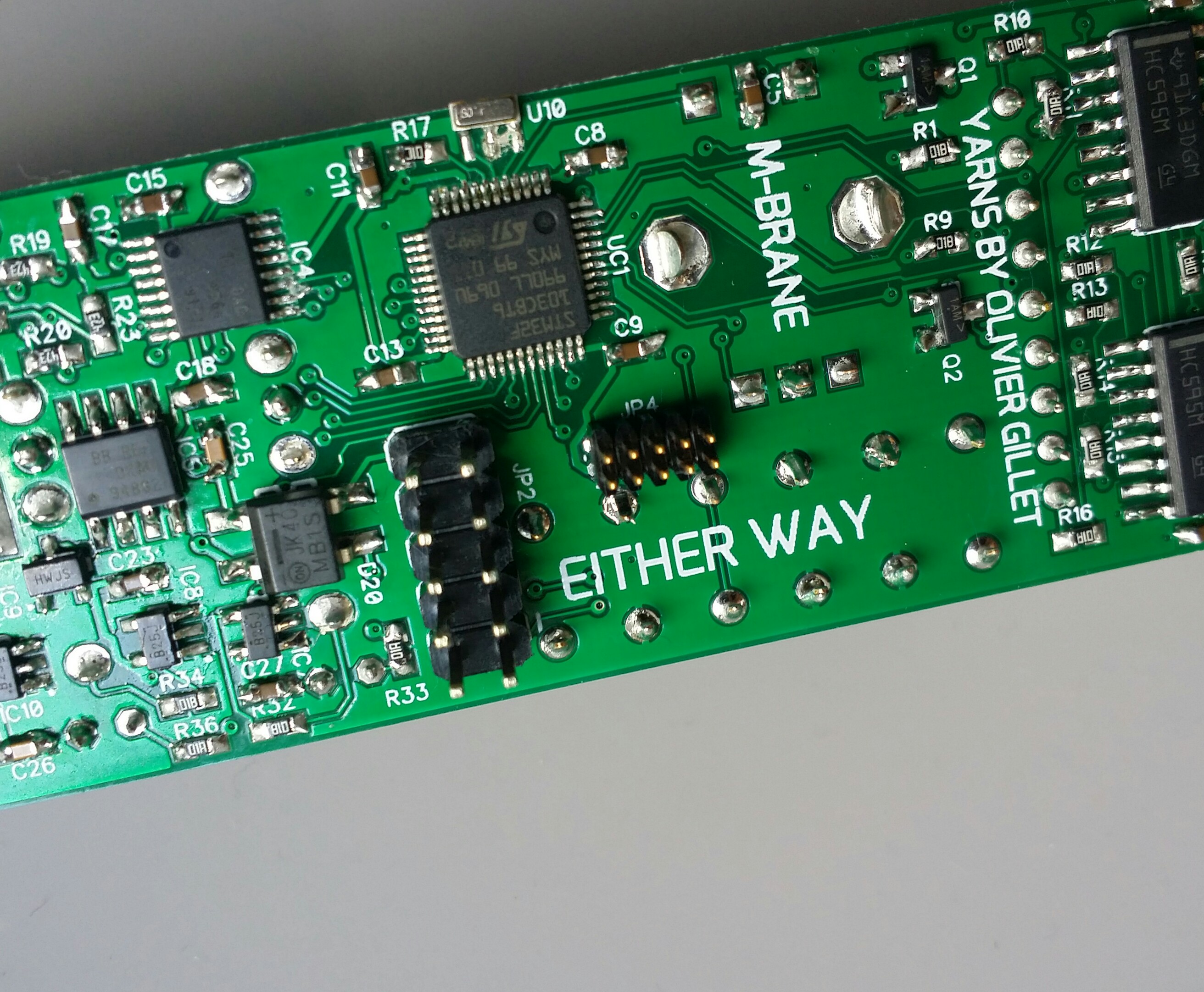
With some fanfare, I plugged the 10-pin power cable in. The PCB helpfully has “Either Way” printed for this, and the power header is thoughtfully protected against reverse-voltage. Powering up the case, all the controls worked as they should, but it would not receive MIDI. There turned out to be two problems. First, the solder I had applied to the ground leg of the optocoupler hadn’t wet the pad. This was particularly annoying to test, since applying probe pressure would bridge the connection, and everything would briefly work: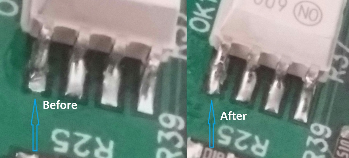
Pretty hard to see, even in the blown up photo. Good object lesson in testing all connections as I go. As penance, I re-tested all the IC legs and found a dodgy connection on one of the gate output buffers, too. The second problem was getting the TRS-MIDI in the right configuration:
5. MIDI Jacks
The Jakplugg Github page explains that there are jumpers on the back that can switch the configuration of the TRS-MIDI connections to either of the two versions. The common ‘Midi Manufacturer’s Association/Korg’ standard sends the MIDI signal on the jack tip, and the ‘Arturia’ standard sends the MIDI signal on the jack ring.
The module requires the ‘Arturia’ signal-on-ring version by default, and the jumpers didn’t seem to help out when I tried to use my Korg MIDI adapter. As far as I can tell, the jumper labeled ‘IN’ only connects the signal pin to BOTH legs of the optocoupler when it is bridged, essentially shorting the MIDI loop across the 220 ohm input resistor. Hmmm.
So anyway, after a lot of testing and confusion I just lopped one end off a spare MIDI cable and soldered a spare headphone plug on there with the signal on the ring and the +3.3V current source on the tip. It works, no adapter necessary.
6. Calibration
The calibration is dead simple, if a bit tedious. Long-click the encoder, select the option, and click through and adjust with the encoder for each single-voltage step from -3V to +7V for each of the 4 CV’s. Click ‘OK’ at the end of each CV channel, and then ‘OK’ again at the end of all of them.
I did the calibration on my digital oscilloscope which reads to single mV – in compliance with the Yarns manual “A multimeter with at least 4 1⁄2 digits of precision”. I think even calibrating with a two-decimal place multimeter would be fine if that’s what is available. At best, I still got a couple mV of drift at each calibration point. In addition, very few of the calibration points were off by less than 50mV to begin with, so just adjusting to halfway between +10mV and -10mV for each point would be significantly better than nothing. And even after calibration, when I rebooted and went through a second time, some of the points were still off by a few mV anyway.
7. Summary
I can’t complain, the module works as intended. There are a few things I might tinker with in the code if I get bored but nothing immediately necessary. Using MIDI with the Clouds module, I think in most cases I would much rather have a third (Octatrack-controlled) LFO instead of velocity, which isn’t an option at the moment.
It would also be nice to have more options for the voltage range of the MIDI-controlled CV outs. Currently, they only do 0 to +5V standard unipolar. My back-of-the-envelope calculations show that the op-amps connected to the DAC (0-5V) are set up for -5.1 gain and +7.6V offset, so in theory there isn’t any reason the CVs can’t swing +/-5 Volts, which would be ideal for controlling the full range of Clouds’ inputs, for example.
The spreadsheet above lists the prices I paid for the parts – about 50€ from Mouser and 55€ from the others including shipping. Considering my next-best option for the same module would have been something like 220€ at least with customs and a massive virus-induced shipping delay, I think I did pretty good. It certainly beats the pants off similarly-specced modules like uMIDI (245€ and too deep for the 4ms pod I’m using anyway), Befaco (254€, also too deep, and a 12-bit DAC…) or 1983(329€!). That only values my estimated 25 hours of labor at somewhere around 4.20€ an hour but what the hell, the first time is for fun.
Still useful in 2023. This info about oscillator polarity saves my time. Thanks!
Thanks for the write-up. What temp are you using for your soldering iron? It looks like either it’s not getting hot enough, you’re using too much solder or not enough flux. You shouldn’t have all of those little peaks of solder coming off of everything. Using some tack flux like Chipquik SMD29130CC will get rid of those completely.
Probably all of the above! 🙂
Thanks for the tip on the Crystal. I am building two, have randomly gotten them both right!
Thanks for saying hi! Good job and have a lot of fun with them!
Thanks for the guide. I’ve got an f103 here and I want to build this.
from lat. manus – “hand” and scribo – “I write”) [1]